MIPAR
  • Products
    • Analysis Software
    • Microscope Software
    • Compliance Software
    • Deep Learning
    • APIs
    • MIPAR for Academics
    • Request a Quote
  • Applications
    • Materials
    • Life Science
    • Manufacturing
    • BioMedical
    • Drone & Survey
    • Recipe Templates
    • Articles & Citations
    • Webinars
  • Spotlight ✧˙˖
  • User Resources
    • Udemy Course
    • Help desk
    • Forum
    • Tutorials
    • FAQ
    • User Manual
  • About
    • Who we are
    • Data Security
    • Newsletter
  • Download Trial
  • Home
  • > 
  • Applications
  •  > 
  • Manufacturing
  •  > 
  • Semiconductors
  •  > 
  • Defects

Semiconductor Defect Analysis with MIPAR

Automating Precision in Semiconductor Quality Control
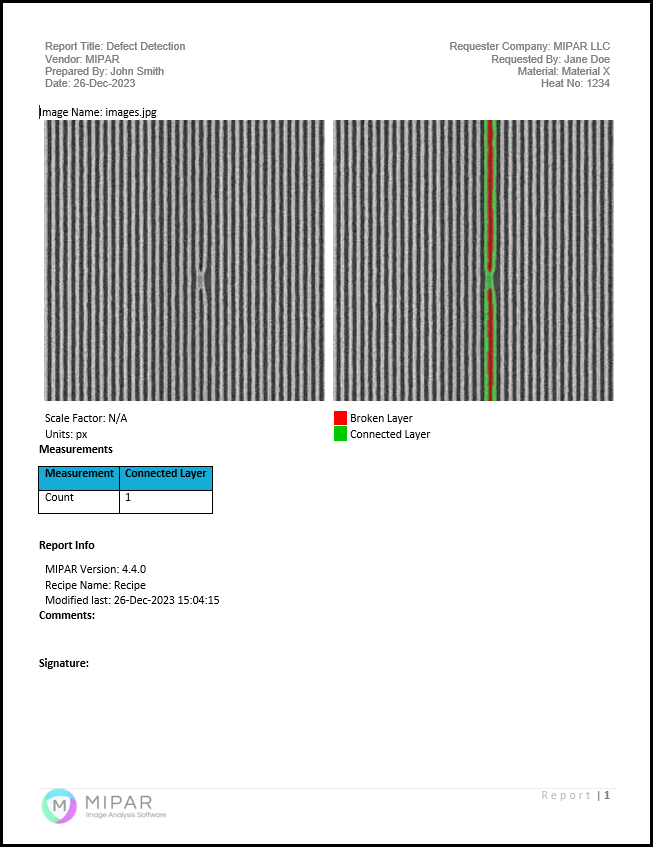
At MIPAR, our goal is to fully automate defect analysis in semiconductor manufacturing, utilizing both fully automated and supervised workflows. Our software streamlines the process of detecting and quantifying semiconductor defects, eliminating the need for manual inspection and increasing accuracy and efficiency in semiconductor quality control.
 
Comprehensive Overview of Semiconductor Defect Analysis
Defect analysis is crucial in semiconductor manufacturing, as even the smallest imperfections can significantly impact the performance and reliability of electronic devices. It involves the examination of semiconductor wafers and chips for flaws such as impurities, dislocations, and fabrication errors. Effective semiconductor quality control ensures that these defects are identified and addressed early in the production process.
 
Overcoming Challenges in Semiconductor Defect Analysis
The complexity of semiconductor devices and the need for nanoscale precision pose significant challenges in defect analysis. Manual inspection methods are not only time-consuming but also prone to errors and inconsistencies. Conventional automated solutions often struggle with the precision required at such small scales and the variety of defect types found in semiconductor manufacturing.
 
MIPAR’s Solution for Semiconductor Defects and Quality Control
MIPAR tackles these challenges using sophisticated Deep Learning models combined with conventional image analysis methods. This approach enables MIPAR to accurately detect a wide range of semiconductor defects rapidly. Our software assists in identifying issues early in the manufacturing process, reducing waste and improving yield, which is crucial for maintaining semiconductor quality control.
 
Advantages of Using MIPAR for Semiconductor Defect Analysis
Incorporating MIPAR in semiconductor defect analysis leads to significant time savings, improved consistency in quality control, and a deeper understanding of the manufacturing process. This allows for more reliable and higher-quality semiconductor products, ensuring that semiconductor defects are minimized and semiconductor quality control is maintained.
 
Who Can Benefit?
MIPAR is ideal for semiconductor engineers, fabrication experts, and quality control professionals who require precise and efficient defect analysis to ensure the highest standards in semiconductor manufacturing.
 
Technical Details
MIPAR supports a broad range of file types from various semiconductor imaging equipment. The software includes advanced calibration and metadata import capabilities, with the ability to process large batches of images. MIPAR operates securely on local workstations, eliminating the need for internet connectivity.

System Requirements
Documentation >>

Demo
Interested in seeing MIPAR's capabilities in semiconductor defect analysis? Schedule a demo with a MIPAR Applications Engineer to discover how our software can enhance the quality and efficiency of your semiconductor manufacturing process.

Support
Our Applications Engineers bring extensive experience in semiconductor processes and automated micrograph analysis. The MIPAR support team is committed to assisting you in achieving excellence in your semiconductor defect analysis efforts.

Cost
License costs vary based on the type of license and the number of users. For detailed pricing information tailored to your semiconductor analysis needs, please submit a quote request. 

QUOTE
Sample Aluminum Grain Size Report

Resources
​​
• Citations
​
• ​The Basics of Semiconductor Defect Analysis

Picture

Check Out Our Products

Picture

MIPAR Base: our core product to analyze images from almost any source. Extensions enable Deep Learning models, Word reports and 3D data analysis.  MIPAR Base Page >>

Picture

​Microscope Software: capture, analyze and report all in a single workflow with MIPAR Live. Check to see if your camera is supported. MIPAR Live Page >> ​​

Picture

Compliance Software: analyze, report, and approve in a 21 CFR Part 11 or GMP Annex 11 compliant environment with traceability. MIPAR Checkpoint Page >> ​​

Picture

MIPAR APIs: tools to help integrate MIPAR detection and measurement solutions into other software applications and workflows. APIs Page >> ​​​

Picture

Call

Give us a call
​Mon-Fri 9am-6pm EST​​
​​+1-614-407-4510

Message

Tell us how we can help!

Chat

Chat with us
​Mon-Fri 9am-6pm EST​​
Chat with us ››

Home

Support

Contact

© 2025 |  Privacy  |  Terms
  • Products
    • Analysis Software
    • Microscope Software
    • Compliance Software
    • Deep Learning
    • APIs
    • MIPAR for Academics
    • Request a Quote
  • Applications
    • Materials
    • Life Science
    • Manufacturing
    • BioMedical
    • Drone & Survey
    • Recipe Templates
    • Articles & Citations
    • Webinars
  • Spotlight ✧˙˖
  • User Resources
    • Udemy Course
    • Help desk
    • Forum
    • Tutorials
    • FAQ
    • User Manual
  • About
    • Who we are
    • Data Security
    • Newsletter
  • Download Trial