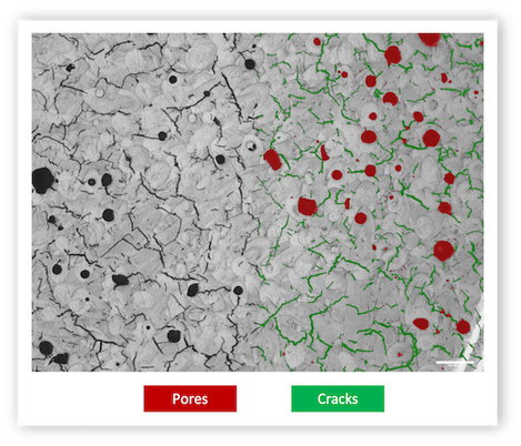
The Digital Evolution of Defect Analysis
Defect analysis usually refers to the task of studying the properties of defects themselves, rather than a technique for predicting the number and nature of defects using advanced software and complexity models. Defect analysis is often the first type of data analysis to be collected as it is a part of continuous quality improvement planning. Subsequent defects are classified into various categories which classifies possible causes in an attempt to prevent problems from occurring.
Why is Defect Analysis Going Digital?
Defect analysis based on critical tools like electron microscopy is an important element of materials science, providing detailed insights regarding the microstructure and performance of a broad variety of materials and material systems. Recent advances in computer vision and machine learning have been introduced into the field of scanning electron microscopy (SEM) for image analysis. It is used for detection and segmentation of medical images, the unsupervised statistical representation of microstructure images, clustering, or classification in a range of material image and local transformation tracking at the atomic level in scanning electron microscopic images.
As scaling continues in scanning electron microscopy (SEM), the industry moves towards sub 1× nm nodes. This means that defect analysis faces increasingly difficult challenges as the defects shrink making their identification and analysis extremely challenging.
Creating a flexible but robust platform for digital defect analysis and recognition in electron microscopy will lead to the completion of analysis orders of magnitude faster following the image recording.
Benefits of Digital Defect Analysis Over Manual
Digital detail analysis is more accurate, efficient, and repeatable than manual, human analysis. It is able to scale with the methods of automated data generation that are growing in importance.
Manual defect analysis can be extremely time-consuming, particularly when there is a large data set of microscopy images. Each image can require anywhere between a few minutes to around an hour per image.
Manual defect analysis is also error prone as it is easy to miss a defect or not identify one correctly. It also inconsistent, lacks reproducibility, and defect analysis can be substantially impacted by human bias and the specific training a researcher has. This makes it more challenging to compare defect analysis results across groups or ascertain absolute behavior.
Manual defect analysis also cannot scale well. Recent innovations in electron microscopes have enabled them to take up to thousands of images per second. Digital defect analysis automates this process, making it a critical element to increasing data generation capacities.
A digital image analysis device could reduce the time required for analysis to close to zero, offering consistent, accurate, unbiased results with the ability to scale.
Digital Defect Analysis from MIPAR

